


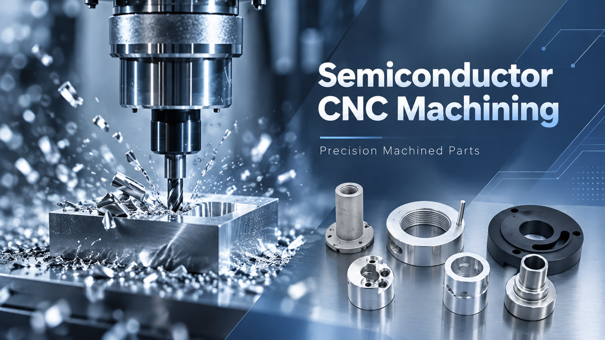
Let’s admit it: CNC machining is rarely the first thing people think about when talking about semiconductor manufacturing. Most attention goes to wafers, chips and lithography. But behind that equipment are countless precision metal and plastic parts that directly affect how reliably the system runs.
They may need to operate for long periods under vacuum, high temperature, corrosive gases or tightly controlled thermal conditions, while still maintaining stable dimensions and reliable positioning.
That level of performance places much higher demands on machining than ordinary industrial parts.
The challenge is not only achieving a tight tolerance. Semiconductor parts may also require good flatness, stable material behavior, clean surfaces, precise feature relationships, low burr levels and consistent repeatability from one production batch to the next.
This is why CNC machining is widely used for semiconductor equipment components. From wafer handling parts and vacuum components to manifolds, cooling plates, housings and precision fixtures, the machining method must match the function of the part.
This guide explains the main semiconductor CNC machining processes, common materials, custom part design, 5-axis machining, distortion control, inspection and the key factors to consider when choosing a semiconductor CNC machining manufacturer.

Key Takeaways
Semiconductor CNC machining covers more than CNC milling. Depending on the part, production may involve CNC turning, Swiss machining, drilling, boring, threading, EDM, grinding and multi-axis machining.
The most important requirements are often not limited to dimensional tolerance. Flatness, positional accuracy, sealing surfaces, cleanliness, burr control and material stability can be equally important.
Aluminum remains one of the most practical materials for semiconductor equipment because it combines machinability, low weight and good thermal conductivity. Stainless steel, copper, titanium and engineering plastics are used where their specific properties are required.
5-axis CNC machining is especially useful when several critical features must remain accurately related to one another. Its main advantage is reducing setups rather than simply producing more complicated shapes.
Custom semiconductor parts should be designed around function. Deep pockets, thin walls, unnecessarily tight tolerances, difficult tool access and poorly defined datums can increase cost and machining risk.
Inspection should also follow function. A sealing surface, locating bore and cosmetic outer wall do not need to be controlled in the same way.
What Is Semiconductor CNC Machining?
Semiconductor CNC machining is the use of computer-controlled machining processes to produce precision mechanical parts for semiconductor manufacturing, inspection, testing and handling equipment.
It is important to separate this from semiconductor manufacturing itself. CNC machines do not produce the chips or create features on the wafer. Instead, they manufacture many of the mechanical components that allow semiconductor equipment to position, process, cool, seal, move and inspect wafers accurately.
These parts can be found throughout lithography systems, vacuum chambers, wafer handling equipment, gas delivery systems, thermal management systems, metrology equipment and semiconductor test machines.
The machining itself may use familiar processes such as milling and turning, but the requirements are often different from normal industrial CNC work. Many components have to maintain reliable performance in vacuum, controlled thermal environments or chemically aggressive conditions, while also meeting strict requirements for dimensional stability, surface quality and contamination control.
So, semiconductor CNC machining is better understood as a specialized form of precision manufacturing rather than simply “CNC machining with tighter tolerances.” The machine tool is only one part of the process. Material behavior, machining strategy, process control and how consistently the finished part performs in the equipment all matter.

Common CNC Machined Parts for Semiconductor Industry
There is no single type of semiconductor CNC machined part.
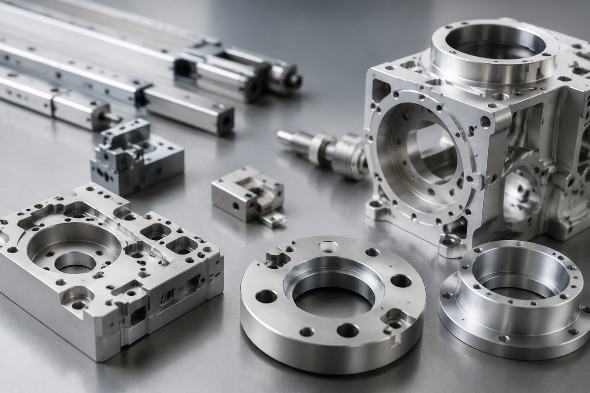
Some parts are large aluminum plates. Others are small turned shafts, vacuum adapters, precision rings or plastic insulating components.
The machining process depends heavily on the equipment system and part function.
| Application Area | Typical CNC Machined Parts |
| Vacuum and process systems | Vacuum chambers, chamber covers, vacuum flanges, adapter plates, gas manifolds, sealing components, process plates |
| Wafer handling systems | Wafer stages, wafer carriers, end effectors, handling arms, alignment plates, positioning components |
| Thermal management systems | Liquid cold plates, cooling blocks, heat spreaders, thermal plates, cooling manifolds |
| Motion and precision positioning systems | Precision shafts, sleeves, bushings, actuator mounts, guide components, positioning brackets |
| Optical and metrology systems | Optical mounts, sensor housings, alignment components, measurement stages, precision fixtures |
| Testing equipment | Test fixtures, probe station components, socket fixtures, inspection fixtures |
| Equipment structures and custom assemblies | Base plates, housings, frames, mounting plates, custom enclosures |
Many of these parts require more than one machining process.
For example, a vacuum adapter may begin as a turned component but later require milled bolt patterns, flats or side ports.
A large chamber plate may require CNC milling, EDM for difficult features and grinding if certain surfaces need very tight flatness.
The process should follow the part, rather than forcing every design into the same CNC machining method.
CNC Machining Processes Used for Semiconductor Parts
CNC Milling
CNC milling is one of the most widely used processes in CNC machining for semiconductor industry applications.
It is suitable for parts such as chamber plates, manifolds, housings, cold plates, fixtures, equipment bases, wafer handling components, optical mounts, or complex brackets.
Milling is especially useful when the component contains pockets, slots, sealing surfaces, locating holes, channels or multiple features distributed across flat or angled surfaces.
Large semiconductor equipment plates may look relatively simple, but machining them can be difficult when a significant amount of material must be removed.
A deep chamber cavity, for example, can release internal stress from the original aluminum stock. The challenge then becomes keeping the remaining structure flat after machining.
For these parts, process sequence matters as much as machine accuracy.
CNC Turning
CNC turning is also an important part of semiconductor machining, especially for cylindrical components.
Typical turned parts include shafts, sleeves, rings, vacuum adapters, cylindrical housings, flanges, threaded fittings, bushings, or precision spacers.
Turning is well suited to controlling concentricity, diameter, bore size and cylindrical sealing surfaces.
A semiconductor component does not necessarily remain a pure turning part.
Consider a custom vacuum adapter.
The OD, ID, sealing face and groove may first be produced on a CNC lathe. The part can then move to a machining center for side holes, bolt patterns, flats or ports.
Turning and milling are often used together when cylindrical components also contain non-rotational features.
For these parts, the important issue is often maintaining the relationship between the turned datum and the later milled features.
Swiss Machining
Swiss machining can be useful for smaller, long or slender semiconductor components.
Typical applications may include small shafts, pins, miniature sleeves, connector-related components, contact components, or precision threaded parts.
The guide-bushing design of Swiss machines supports the material close to the cutting area, which helps control deflection when machining small-diameter components.
For high-volume miniature components with several turning and milling features, Swiss machining can also reduce the need for multiple separate operations.
It is not required for every small semiconductor part, but it can be an efficient option when geometry and production volume justify it.
Drilling, Boring, Reaming and Threading
Small machining operations can have a major effect on semiconductor equipment assembly.
Drilling is widely used for mounting holes, fluid channels, gas ports and threaded interfaces.
Boring and reaming are more suitable when a hole requires better diameter control, roundness or positioning than a standard drilling operation can provide.
Threading is also common in vacuum interfaces, equipment assemblies, fluid connections, covers, manifolds, mounting structures.
Thread specifications should be selected according to the actual interface.
Very small or unnecessarily deep threaded holes increase manufacturing risk without always providing additional functional value.
5-Axis CNC Machining for Semiconductor Parts
For semiconductor components, 5-axis CNC machining is mainly valuable when multiple precision features need to be machined from different directions while maintaining their relationship to the same datum.
Many semiconductor parts, such as vacuum components, manifolds, wafer handling parts and precision fixtures, may include angled surfaces, side ports, complex cavities or multiple mounting features. With traditional machining, these features often require several setups, and every repositioning operation can introduce alignment variation.
By reducing the number of setups, 5-axis machining helps improve feature-to-feature accuracy, simplify fixturing and maintain better consistency for complex parts.
Key advantages of 5-axis machining include:
-
Fewer setups: Reduce repositioning errors when machining multi-face components.
-
Better tool access: Reach angled features and complex areas with a more suitable cutting direction.
-
Improved machining stability: Shorter tool reach can reduce vibration and tool deflection.
-
Greater design flexibility: Suitable for complex manifolds, chamber components, cooling parts, optical mounts and precision fixtures.
Compared with 3-axis CNC machining, 5-axis machining is more suitable for complex, multi-face components, while 3-axis machining remains a practical choice for simpler parts such as flat plates, standard brackets and basic housings.
| Consideration | 3-Axis CNC | 5-Axis CNC |
| Simple plates and pockets | Excellent choice | Usually unnecessary |
| Multi-face features | More setups required | Fewer setups |
| Angled features | Additional fixtures may be needed | Better accessibility |
| Complex geometries | Limited | Strong advantage |
| Setup-related variation | Higher | Lower |
However, 5-axis machining is not always the best solution. For simple semiconductor components with straightforward geometry, a well-controlled 3-axis process can often achieve the required accuracy at a lower cost.
The right machining method depends on the part geometry, tolerance requirements and functional needs, not simply the number of machine axes.
Why Semiconductor CNC Machining Is More Demanding
Semiconductor components are often associated with extremely tight tolerances, but dimensional accuracy is only one part of the challenge.
A part can meet its basic dimensions and still fail in the final application if its flatness, surface condition, material stability or feature relationship is not properly controlled.
Compared with general industrial CNC parts, semiconductor components often require additional control in several areas:
| Requirement | Why It Matters |
| Dimensional accuracy | Ensures proper assembly and positioning |
| Flatness and parallelism | Important for sealing, mounting and thermal contact |
| Feature relationship | Keeps holes, surfaces and interfaces aligned correctly |
| Material stability | Reduces deformation during machining and operation |
| Surface condition | Affects sealing, friction and equipment performance |
| Burr and contamination control | Helps reduce particle-related risks |
| Repeatability | Ensures consistent performance across production batches |
The key difference is that semiconductor CNC machining focuses not only on producing a part that matches the drawing, but also on producing a part that performs reliably inside a highly controlled equipment environment.

Materials Used for Semiconductor CNC Machined Parts
Material selection should begin with the application.
Temperature, corrosion, vacuum compatibility, electrical behavior, weight, wear and thermal conductivity all influence the choice.
Aluminum
Aluminum is one of the most common materials used for semiconductor equipment structures and precision components.
6061-T6 is popular because it provides a practical balance of machinability, dimensional stability, corrosion resistance and cost.
Common semiconductor applications include:
-
chamber components
-
wafer stages
-
equipment plates
-
housings
-
fixtures
-
heat sinks
-
cold plates
-
vacuum components
Aluminum also machines much faster than many stainless steels or titanium alloys.
The main issue is distortion.
When a large pocket is removed from a thick aluminum block, the remaining structure can move as internal stresses are released.
Thin walls and heavily pocketed plates are especially sensitive.
For this reason, high-precision aluminum machining may involve rough machining first, leaving finishing stock, allowing the part to relax, and then performing the final machining operation.
That extra process can be more valuable than simply running the machine more slowly.
Stainless Steel
Stainless steel machining for semiconductor parts is common where corrosion resistance, strength, durable threads or wear resistance are important.
Grades such as 304 and 316L may be used for:
-
vacuum hardware
-
fittings
-
fixtures
-
structural components
-
fluid-handling parts
-
precision adapters
Compared with aluminum, stainless steel normally creates higher cutting forces and more heat.
Tool wear, work hardening, chip control and fixturing therefore become more important.
It may also make little economic sense to specify stainless steel for the entire component when only one interface requires its wear or corrosion resistance.
Material selection should follow the real operating environment.
Copper
Copper is useful when thermal or electrical conductivity is the main design requirement.
Applications can include:
-
heat-transfer components
-
cooling parts
-
electrical interfaces
-
power-related parts
-
specialized fixtures
Copper looks easy to machine because it is soft, but that softness creates its own problems.
Material can smear around small features. Burrs can form around drilled holes or narrow channels.
Thin structures may also deform if the cutting strategy is not controlled.
Sharp tooling and careful burr management are therefore important.
Titanium
Titanium is less common than aluminum or stainless steel in general semiconductor equipment, but it can be useful where corrosion resistance, strength and low weight justify the higher material and machining cost.
It is much more demanding to machine than aluminum.
Heat remains concentrated near the cutting edge, which accelerates tool wear.
Cutting parameters, cooling and tool engagement must therefore be controlled carefully.
Titanium should normally be selected because the application requires its properties, not simply because it is considered a higher-performance material.
Plastic
Semiconductor plastic machining is important for components that need electrical insulation, chemical resistance, low weight or specific thermal and vacuum-related properties. Common materials include PEEK, PTFE, POM, engineering nylon, other application-specific plastics.
PEEK is often selected where temperature resistance, chemical resistance and dimensional stability are important.
PTFE offers excellent chemical resistance but is much softer and more difficult to hold to tight dimensional tolerances.
Plastic machining requires a different approach from metal machining.
Heat generated during cutting can change dimensions temporarily.
Excessive clamping force can distort the blank.
Soft materials can also produce burrs or damaged edges if cutting parameters are not appropriate.
For semiconductor plastic parts, material behavior and tolerance requirements should therefore be considered together.
Semiconductor CNC Machining Design Considerations
Good part design has a direct impact on machining accuracy, production cost and long-term consistency. For semiconductor components, engineers should consider not only the final geometry, but also how the part will be machined, inspected and used in the equipment.
Define Critical Features and Tolerances
Not every dimension on a semiconductor part requires the same tolerance level.
Critical features such as sealing surfaces, locating holes and alignment interfaces should receive tighter control, while non-functional areas can often use standard machining tolerances.
Clear tolerance requirements help avoid unnecessary machining costs and make the manufacturing process more stable.
Use Proper Datums and GD&T
Semiconductor components often depend on the relationship between multiple features rather than individual dimensions.
A clear datum structure and appropriate GD&T requirements help control:
-
hole position
-
flatness
-
parallelism
-
perpendicularity
-
feature alignment
This reduces tolerance stack-up during assembly.
Consider Wall Thickness and Deep Features
Thin walls and deep pockets can create machining challenges.
Thin sections may deform under cutting forces, while deep cavities may require longer tools that increase vibration and reduce stability.
Where possible, designs should allow sufficient material thickness and reasonable tool access.
Plan for Material Removal and Distortion
Large semiconductor parts, especially aluminum plates, chamber components and cooling plates, may experience deformation when significant material is removed during machining.
Machining strategy should be considered during design, including roughing allowance, finishing sequence and potential stress-related movement.
For parts with large pockets or thin remaining walls, removing too much material too quickly can release internal stress and affect flatness after machining. A proper machining sequence, stable fixturing and controlled finishing process help maintain the final geometry after the part is released from the machine.
Consider Surface Finish and Manufacturing Processes
Surface requirements should match the function of the part.
Sealing areas, thermal interfaces, sliding surfaces and cosmetic areas may require different finishes.
Designers should also consider the impact of anodizing, plating or other finishing processes on final dimensions.
Inspection for Semiconductor CNC Machining
Inspection should answer one question:
Does this part meet the functional requirements defined by the drawing?
A CMM is useful for checking complex geometric relationships, hole locations, profiles and datums.
Other tools may be better for surface roughness, bore dimensions or simple production checks.
| Inspection Method | Typical Use |
| CMM | GD&T, location, profile and complex geometry |
| Height gauge | heights and basic positions |
| Micrometer | thickness and external dimensions |
| Bore gauge | precision internal diameters |
| Optical measurement | small or difficult-to-contact features |
| Surface roughness tester | Ra and surface texture |
| Gauge / fixture | repeat production checks |
For a new component, First Article Inspection can be useful.
Depending on customer requirements, the inspection package may also include dimensional report, ballooned drawing, material certificate, surface treatment certificate, and batch information.
CNC Machining vs Other Manufacturing Processes for Semiconductor Parts
Semiconductor equipment components often require a balance between precision, flexibility and production volume. CNC machining is widely used in semiconductor equipment, but it is not the only manufacturing option.
| Process | Suitable Applications | Main Considerations |
| CNC Machining | Custom chambers, manifolds, fixtures, precision plates and complex equipment parts | High flexibility, tight tolerance, suitable for low and medium volumes |
| Die Casting | Higher-volume aluminum housings or mature designs | Requires tooling investment and design stability |
| Sheet Metal Fabrication | Covers, brackets and simple enclosures | Limited for complex precision features |
| Additive Manufacturing | Rapid development or complex internal structures | Material properties and surface finish may require additional processing |
| Grinding / EDM | Secondary operations requiring very tight geometry or difficult features | Usually combined with CNC machining |
In many semiconductor applications, the final solution is not a single process. A component may combine CNC milling, turning, grinding, EDM or finishing operations depending on its functional requirements.
For custom semiconductor CNC machined parts, the best manufacturing method depends on geometry, material, tolerance, quantity and long-term production needs.
How to Choose a Semiconductor CNC Machining Manufacturer
Choosing a semiconductor CNC machining manufacturer should go beyond checking machine lists and claimed tolerances. A reliable supplier should understand both the drawing and the function of the part.
Before production, the supplier should be able to review potential manufacturing risks, including tolerance relationships, thin walls, distortion, tool access, datum strategy, finishing effects, cleaning requirements and inspection methods.
Process capability is also important. Depending on the component, semiconductor machining may require more than CNC milling, including CNC turning, 5-axis machining, grinding, EDM, engineering plastic machining, finishing coordination and dimensional inspection.
Good communication is equally important. A capable supplier should identify potential issues early, such as unstable tolerances after finishing, difficult-to-machine features or inspection challenges, rather than discovering problems after production.
The right manufacturing partner helps ensure semiconductor parts are not only produced accurately, but also manufactured consistently for long-term equipment performance.
Semiconductor CNC Machining at XY-GLOBAL
XY-GLOBAL provides custom semiconductor CNC machining services for precision components used in wafer processing, vacuum systems, thermal management, testing equipment and other semiconductor applications.
Our capabilities cover CNC milling, CNC turning, 5-axis machining, EDM, grinding and engineering plastic machining, supporting materials including aluminum, stainless steel, copper, titanium and technical plastics.
Before production, our engineering team supports DFM, reviews part geometry, material selection, machining strategy and inspection requirements to improve manufacturing stability. We have the capability to machine various semiconductor components, from small precision parts to larger equipment structures, with stable process control for complex geometries and tight-tolerance features.
For quality control, XY-GLOBAL uses CMM inspection equipment with measurement capability down to 0.001 mm and supports dimensional reports, material traceability and process documentation when required. XY-GLOBAL operates under ISO 9001 quality management systems, supporting rapid prototyping, stable and repeatable manufacturing for precision semiconductor components with fast lead time.
If you have a semiconductor equipment component, send us your 2D drawing and 3D model. Our engineering team can review the material, machining process, tolerance, geometry and inspection requirements before production.
Frequently Asked Questions for Semiconductor CNC Machining
1. Which aluminum is commonly used for semiconductor equipment parts?
6061-T6 is widely used because of its machinability, strength, corrosion resistance and thermal performance.
Other aluminum grades may be selected when greater strength or different physical properties are required.
2. Can CNC machining be used for custom semiconductor equipment parts?
Yes. Many semiconductor components are application-specific and manufactured according to customer drawings or CAD models.
CNC machining is suitable for custom parts because it provides design flexibility without requiring expensive production tooling, making it practical for prototypes, low-volume production and repeat manufacturing.
3. What quality documents are usually required for semiconductor CNC machining?
Depending on the project requirements, customers may request dimensional inspection reports, material certificates, traceability records, first article inspection (FAI) reports and other manufacturing documentation.
A reliable supplier should be able to provide clear quality records for critical components.
4. How can semiconductor CNC machining suppliers reduce contamination risks?
Contamination control involves more than final cleaning. Suppliers should consider material selection, machining processes, burr removal, chip control, surface requirements and cleaning methods, especially for vacuum-related or sensitive equipment components.
5. What information should I send for a semiconductor CNC machining quote?
A 3D CAD model and 2D drawing are ideal. Include material, quantity, tolerances, GD&T, surface requirements, finishing, inspection requirements and any special cleaning or packaging requirements.

分享:
Custom Die-Casting Mold Manufacturer Focused on Longer Tool Life
How Ultra Precision Diamond Turning Enables True 0 Tolerance CNC Machining