XY-Global specializes in on-demand manufacturing for the semiconductor device industry, offering competitive pricing and deep expertise in semiconductor parts manufacturing. Our commitment to excellence ensures that critical components are produced reliably and cost-effectively to meet the industry's most demanding standards.
High-precision semiconductor equipment parts
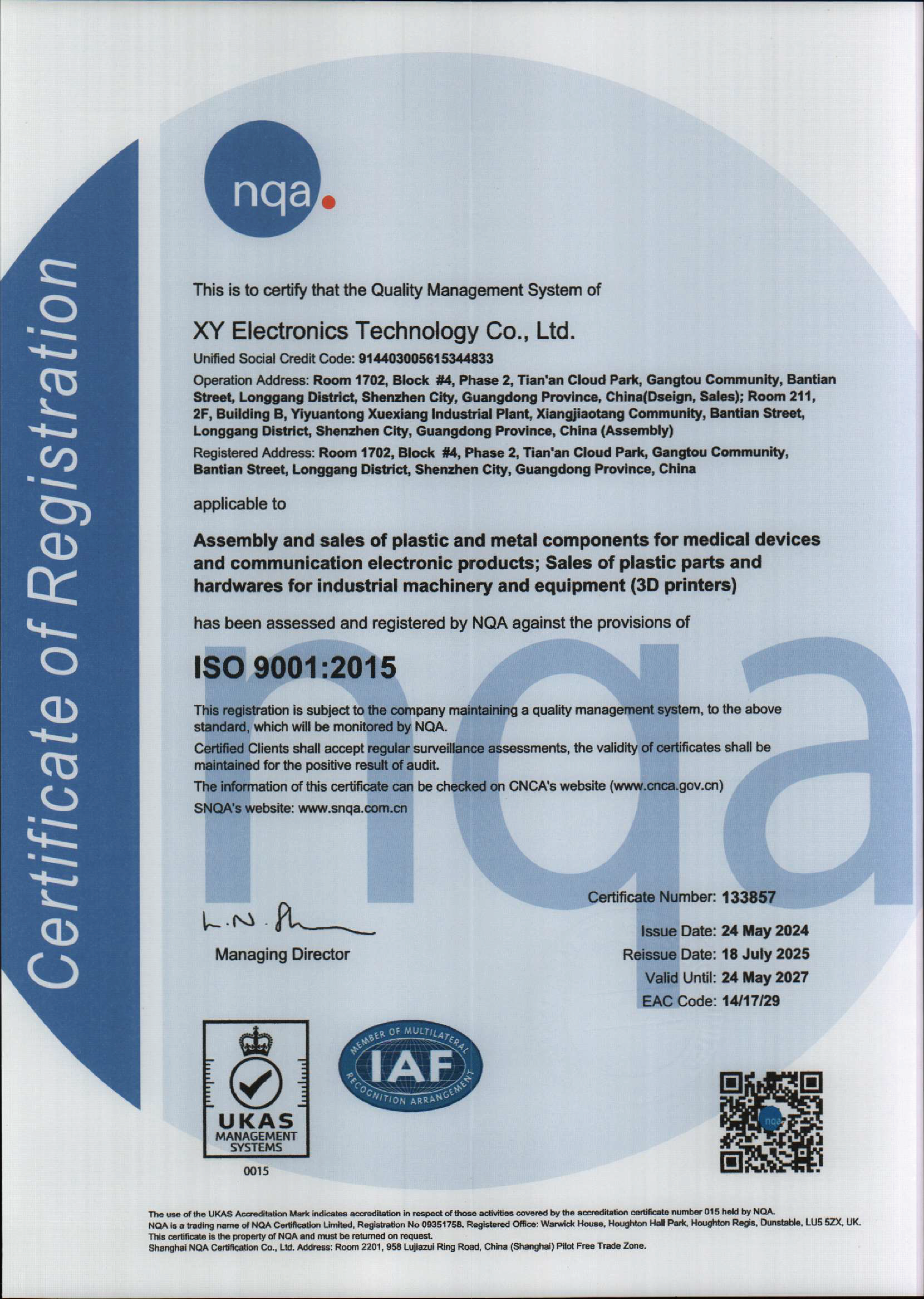
ISO 9001 certified
24/7 engineering support
Precision Machined Components In Semiconductor Manufacturing
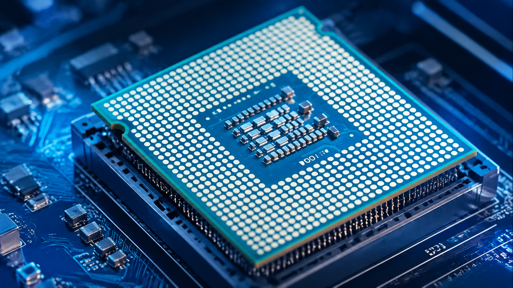
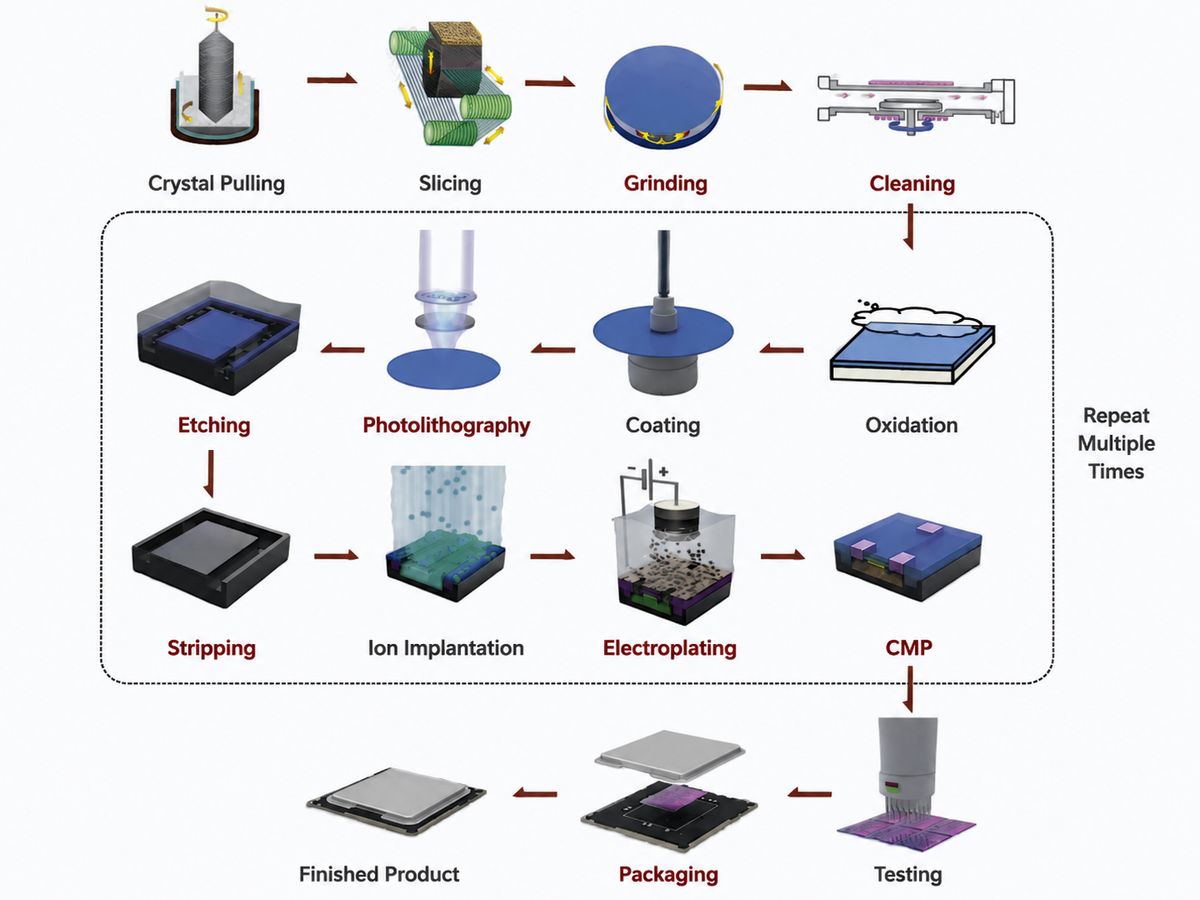
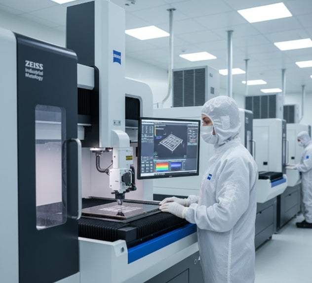
The semiconductor manufacturing process involves highly precise steps such as wafer fabrication, lithography, etching and inspection. Each stage requires advanced equipment with excellent accuracy, stability and cleanliness.
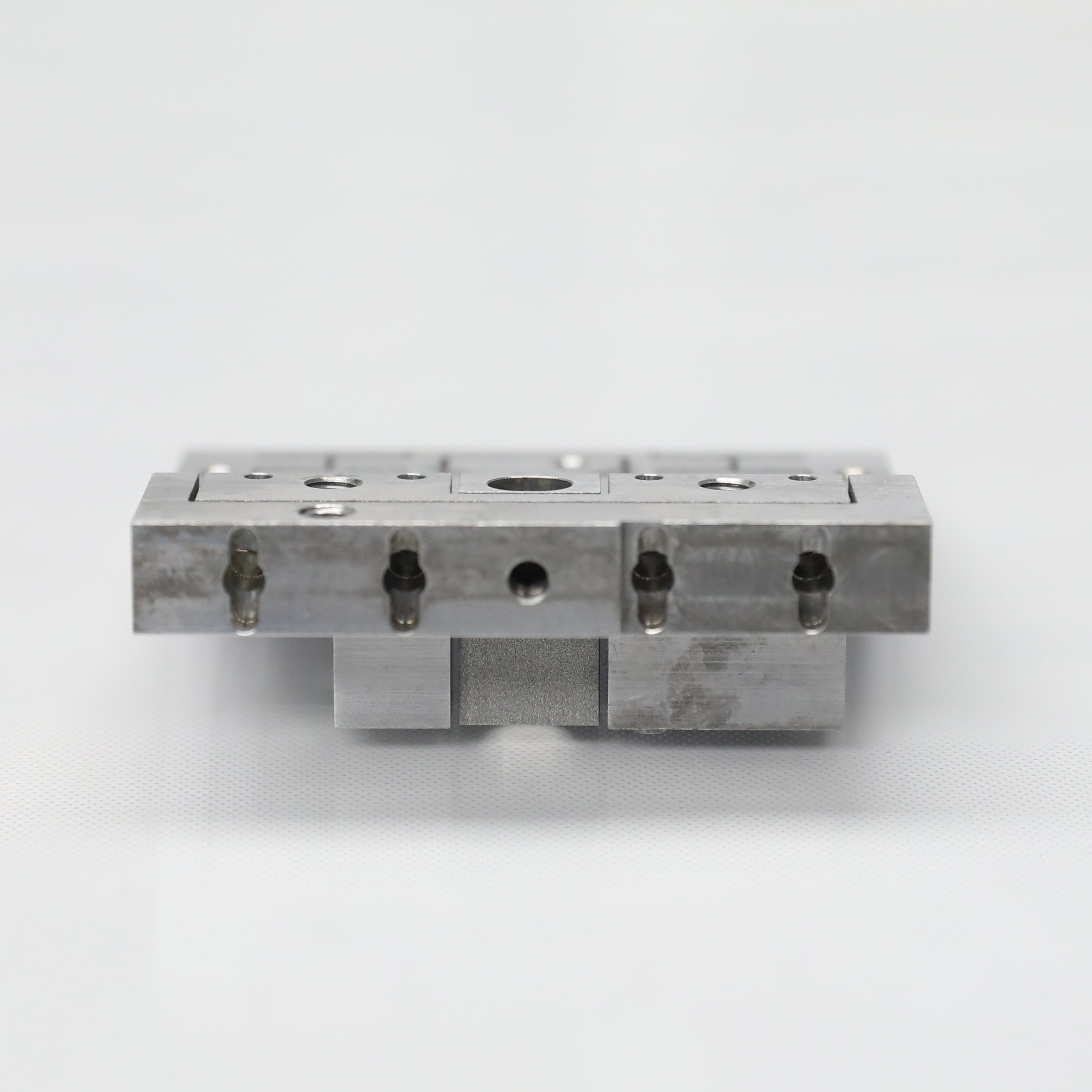
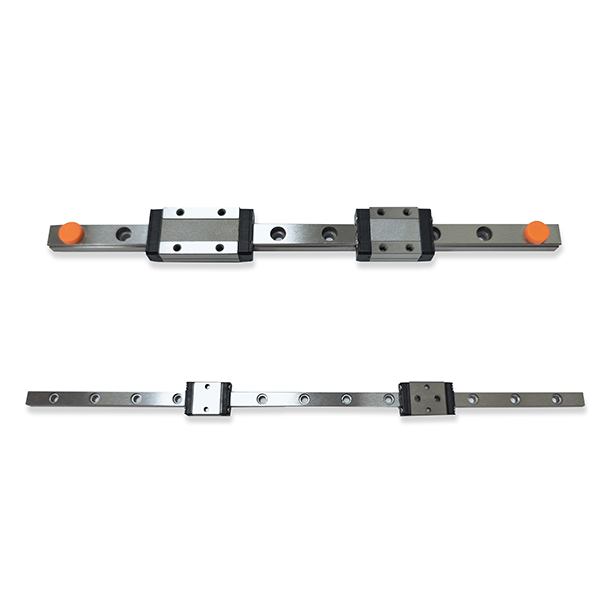
At XY-GLOBAL, we do not manufacture semiconductor chips or wafers. Instead, we support semiconductor equipment manufacturers by providing precision machined components used in these advanced systems.Our capabilities include manufacturing precision brackets, mounting plates, chamber components and custom mechanical parts with tight tolerances, reliable quality and consistent performance.
Comprehensive Semiconductor Application Expertise
Our extensive production capabilities enable us to enhance semiconductor device manufacturing across various technological applications. Our expertise includes:
Fabrication & lithography: Photomasks for semiconductor fabrication and photomask precision-cut plates.
Power & discrete devices: Metal brackets for rectifiers and precision metal components for field-effect transistors.
Packaging & solar technology: Lead frames for semiconductor packages and precision metal frames for solar cell panels.
ISO 9001 Certified Quality
XY-Global is an ISO 9001 certified supplier, ensuring all optical prototypes and components meet comprehensive regulatory requirements. Our rigorous quality control systems guarantee that every part meets your specific needs. We are ready to serve you!
Why Choose XY-GLOBAL for Parts in Semiconductor Industry
Certified Quality & Semiconductor Compliance: ISO 9001 certification ensures all semiconductor components meet strict standards for material purity and mechanical integrity.
Sub‑Micron Precision Machining: Our CNC technology achieves tolerances as tight as 1 µm, meeting the extreme accuracy required for wafer handling and lithography systems.
Seamless Prototyping to Production: We provide a smooth transition from prototypes to low‑volume production, enabling rapid design validation and efficient scaling.
Specialized Materials & Custom Tooling: We use advanced alloys and custom tooling to meet the harsh thermal, chemical, and mechanical demands of semiconductor fabrication.
AI‑Driven DFM & Faster Time‑to‑Market: Our digital platform delivers instant quotes and automated DFM feedback, while high‑speed manufacturing cuts lead times by up to 50%.
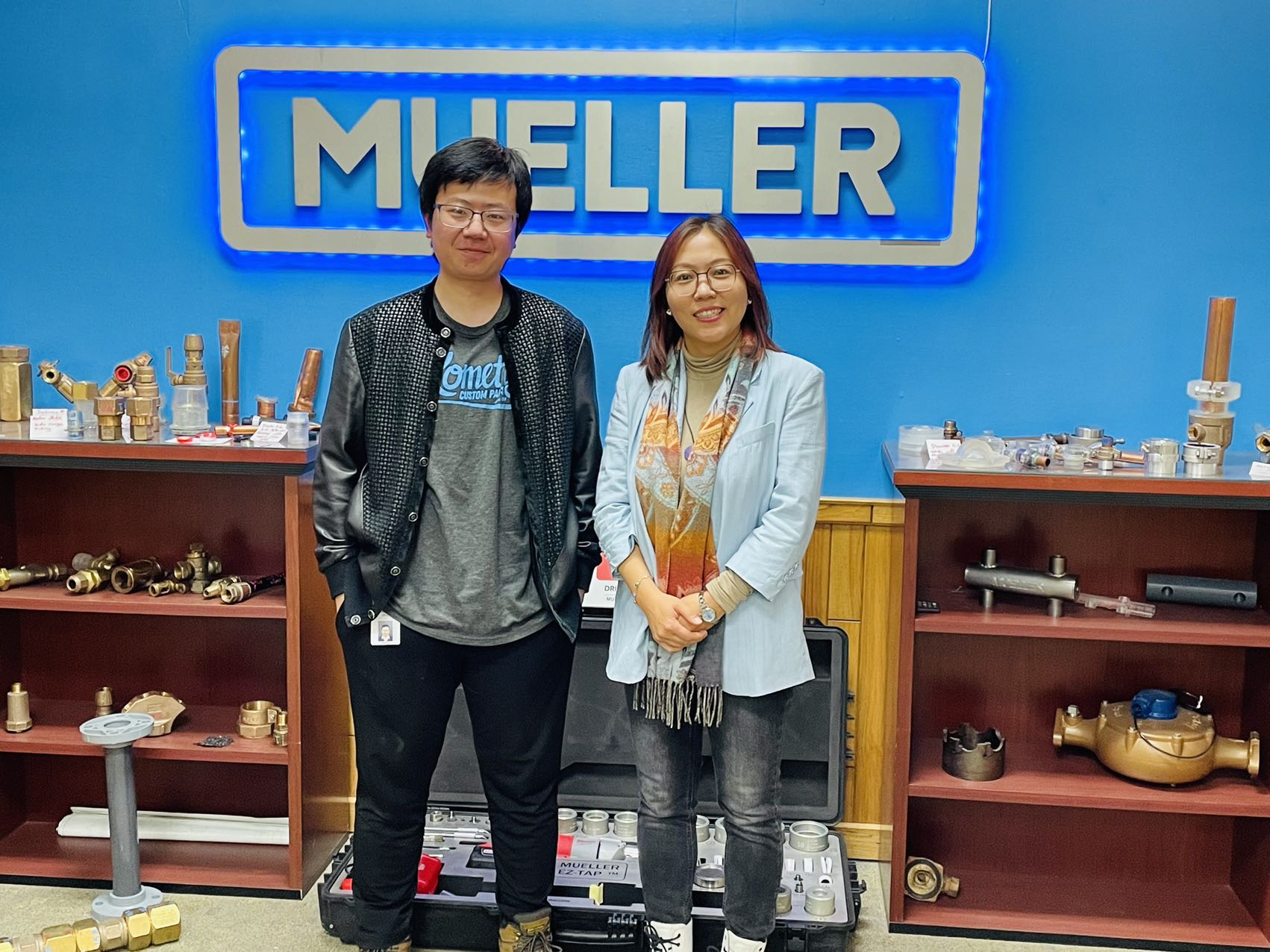
Dear XY-Global Ivy,
Thank you for your visit with me at Mueller Co. located at Decatur, IL on 12/06/2022, and thank you for your continuous support to our new product development process. I hope to work with you on future projects with trust on your quality control, good service, and customer support!
— Ethan, Yixin Lifrom Mueller Co.
Choosing a selection results in a full page refresh.