


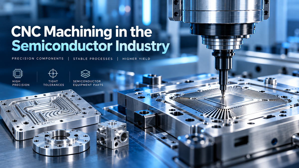
Let's face it. CNC machining in the semiconductor industry often means tight tolerances, 5-axis machines, and micron-level precision. Those things matter, of course. But they do not tell the whole story.
A semiconductor equipment part can pass dimensional inspection and still cause trouble during assembly or operation while a sealing face may meet its roughness requirement but still have a local scratch. Locating holes may all be the correct size, yet their relationship to the main datum can still be wrong.
Here’s the thing: semiconductor equipment depends on the part working as a system, not on individual dimensions looking good on an inspection report.
That is what makes CNC machining for semiconductor equipment different from ordinary precision machining. The challenge is to keep geometry, material stability, surface condition, cleanliness, and inspection requirements under control at the same time.

What Makes CNC Machining Different in the Semiconductor Industry?
Many general mechanical parts are accepted once the main dimensions fall within tolerance. Semiconductor equipment components often have another layer of requirements because a single machined part may also act as a mounting reference, vacuum interface, thermal contact surface, optical support, fluid manifold, or precision positioning structure.
That means several characteristics can affect function at the same time.
| Requirement | Why It Matters |
| Flatness | Affects sealing, mounting, and thermal contact |
| Feature Position | Controls assembly and alignment |
| Parallelism | Maintains relationships between mating surfaces |
| Surface Condition | Can affect sealing and contact performance |
| Burr Control | Helps reduce contamination and assembly problems |
| Dimensional Stability | Keeps geometry consistent after machining |
| Repeatability | Helps multiple assemblies behave consistently |
Tight Dimensions Do Not Always Mean a Functional Part
Consider a machined semiconductor baseplate with a nominal thickness of 20 mm.
Several measurement points may all fall inside the thickness tolerance. On paper, the result looks good. The plate, however, may still have a slight bow across its full length.
For a simple cover, that may not matter much. For a vacuum sealing surface, optical platform, precision stage, or thermal interface, it can become the main problem.
The same applies to holes. Two locating holes can both have the correct diameter, but the distance and orientation between them may still be wrong for the mating assembly.
This is where geometric control becomes more useful than simply tightening every ± dimension.
GD&T helps define how a feature must relate to another surface or datum. In semiconductor components, flatness, true position, parallelism, perpendicularity, and profile are often more meaningful than a general size tolerance because they describe the relationships that actually affect assembly.
ASME Y14.5 provides the standard framework for defining these geometric relationships on engineering drawings.
In practice, the goal is not to make every feature as tight as possible. The goal is to identify which features control function and tighten those where necessary.
Residual Stress Can Move a Part After Machining
Large aluminum parts are common in semiconductor equipment because aluminum is lightweight, easy to machine, and useful for thermal management.
But large aluminum plates can also be difficult to keep flat.
The raw material already contains residual stress from rolling, extrusion, heat treatment, or previous processing. Once machining starts removing material, that stress balance changes.
Think of a large plate with a deep pocket. A substantial amount of aluminum is removed from one side while relatively thin walls remain around the outside. During machining, the fixture holds the part in place, so everything may look stable.
Then the part is released. It can move.
The result may be bowing, twisting, or loss of flatness even though the machine followed the programmed toolpath accurately.
This is one of the reasons machine accuracy and finished-part stability are not the same thing.
| Process Factor | Possible Result |
| Heavy material removal from one side | Bowing or twisting |
| Excessive clamping force | Shape changes after release |
| Thin remaining walls | Greater sensitivity to stress |
| Finishing critical faces too early | Geometry moves later |
| Uneven stock removal | Higher distortion risk |
A more stable process often leaves enough material for later finishing instead of trying to reach final size immediately after roughing. Critical surfaces may be finished only after the part has gone through the major material-removal stages and had time to stabilize.
The exact sequence depends on the material condition, geometry, wall thickness, and tolerance. There is no single recipe.
Temperature Can Affect Precision More Than It Seems
Temperature is easy to overlook because it is not always visible on the drawing.
For dimensional measurement, the standard reference temperature is 20°C under ISO 1. That matters because metals expand and contract as temperature changes.
For small parts with loose tolerances, the effect may be minor. On a large precision semiconductor baseplate, it can become measurable.
Aluminum is especially sensitive compared with many steels. If a large aluminum plate is inspected while it is still warm from machining, its measured dimensions can differ from the same part after it reaches a stable temperature.
That does not mean every semiconductor component needs a laboratory environment. But measurement conditions become more important as part size increases and tolerances become tighter.
Sure, not every dimensional shift is caused by machining error. Sometimes the part, machine, and inspection environment were simply at different temperatures.
This is also important when different materials are assembled together. Aluminum, stainless steel, copper, and engineering plastics do not expand at the same rate, so thermal behavior can influence alignment and contact in the final equipment.
Surface Roughness Is Only Part of the Surface Story
Ra is useful, but it does not tell you everything about a functional surface.
A sealing face may meet the specified Ra value and still contain a local scratch. Another surface may look very smooth over a small measurement area but still have enough overall waviness to reduce real contact.
Surface texture and surface geometry are not the same thing.
For semiconductor equipment, that distinction matters. For example, a vacuum sealing surface may need good flatness as well as freedom from scratches; a thermal interface depends on contact across a useful area, and a precision mounting face may depend more on orientation and flatness than on an extremely low Ra value.
This is why one general surface-finish note is rarely enough to describe every important surface on a semiconductor component.
Burrs and Internal Particles Can Become Functional Defects
Burrs are common in CNC machining, but the consequence of leaving one behind depends heavily on the application.
An external burr is usually easy to see and remove. Internal burrs are more difficult.
Cross-drilled holes, intersecting passages, threaded ports, coolant channels, and blind features can create areas that are difficult to inspect after machining.
A small burr may stay attached during inspection and break free later. Chips can also become trapped inside the component if cleaning is not planned around the internal geometry.
That makes burr control part of the machining strategy rather than just a final cleanup step.
Drilling direction, breakthrough conditions, machining order, tool choice, and access for deburring can all influence the result. If a difficult internal intersection will become inaccessible later, it is better to address it earlier in the process.
For semiconductor equipment, a part can be dimensionally correct and still be unsuitable because of a loose particle in the wrong place.
The Datum Strategy Should Match the Way the Part Is Assembled
Datums should reflect how the component works in the final assembly.
Suppose the bottom surface of a baseplate is the actual mounting reference. Several locating holes, side ports, and upper mounting features may all depend on that surface.
If those critical features are machined from unrelated setups without a consistent reference, small datum-transfer errors can accumulate.
This is also where machine configuration starts to matter.
A 5-axis machine can be valuable when important features sit on several faces of the same component. The main advantage is not simply that the machine has five axes. It is that related features can sometimes be completed with fewer setup changes.
Every additional setup creates another opportunity for alignment error.
That does not mean every semiconductor part requires 5-axis machining. A simple 3-axis process may be completely suitable. In other cases, 3+2 machining is enough.
The machining strategy should follow the feature relationships, not the idea that more axes automatically mean better quality.
Different Materials Create Different Machining Risks
Semiconductor equipment uses a wide range of materials, and the same tolerance does not mean the same machining difficulty on every material.
| Material | Typical Machining Concerns |
| Aluminum | Residual stress, burrs, scratches, flatness |
| Stainless Steel | Heat, work hardening, tool wear, cutting force |
| Copper | Burr formation, smearing, surface damage |
| Engineering Plastics | Thermal expansion, creep, clamping distortion |
Aluminum gets most of the attention because it is widely used in semiconductor equipment, especially for baseplates, chambers, cooling components, and structural parts.
Stainless steel behaves differently. Cutting forces are higher, work hardening can become a problem, and heat generation can affect tool life and part stability.
Copper introduces another set of issues. It is soft, highly conductive, and can produce difficult burrs. Aggressive clamping can also damage the surface.
Engineering plastics can be even more sensitive to clamping and temperature. A thin polymer feature may deform while held in the fixture and then recover after release.
So a generic statement such as “we can hold ±0.01 mm” does not tell the whole story.
The achievable result depends on material, geometry, feature size, wall thickness, setup, and inspection method.
Inspection Should Follow the Function of the Feature
CMM inspection is valuable in semiconductor machining, but not every quality question should be answered with the same inspection method.
Different features need different checks.
| Feature | What Usually Needs to Be Verified |
| Locating Hole | Diameter, true position, datum relationship |
| Sealing Surface | Flatness, local damage, groove geometry |
| Thermal Interface | Flatness, contact geometry, surface condition |
| Multi-Face Features | Position and orientation relationships |
| Cosmetic Surface | Visual condition and specified finish |
A CMM is well suited to feature relationships and GD&T. A roughness instrument answers a different question. Visual inspection still matters when scratches, edge damage, or handling marks could affect the part.
No single inspection result proves that the entire component will function correctly.
The better approach is to identify which characteristics affect performance and choose the inspection method around those characteristics.
This also avoids over-inspection. Measuring every non-critical surface to the same level does not automatically improve quality.
Drawings Should Make the Design Intent Clear
A good drawing helps the manufacturer understand where precision really matters.
Applying the tightest tolerance everywhere may feel safe, but it can increase machining cost and inspection time without improving the actual assembly.
For semiconductor components, the drawing should clearly identify the critical information:
-
functional datums;
-
sealing or thermal contact surfaces;
-
important GD&T requirements;
-
special burr or cleanliness requirements;
-
critical surface conditions;
-
required inspection records where necessary.
The supplier should not change the customer's functional requirements, but they can point out when a tolerance, datum structure, inaccessible feature, or machining sequence may create unnecessary manufacturing risk.
Let’s be honest, finding that problem before machining is much cheaper than finding it after a batch has already been completed.
CNC Machining for the Semiconductor Industry at XY-GLOBAL
Founded in 2010, XY-GLOBAL has been a one-stop on-demand manufacturer for customers worldwide and well received for precison custom parts with consistent quality and reliale performance under ISO 9001:2015 and ISO 13485:2016 certifications. From 3-axis to 5-axis CNC milling, from DFM support to precision CMM inspection, from various materials to custom designs and solutions, we are just 24/7 there ready to meet the demand.
Semiconductor cnc machining not just means producing qualified parts. For semiconductor projects, our team, pays close attention to flatness, dimensional stability, datum relationships, multi-face alignment, burr control, surface protection, and inspection planning. Just everything about the parts from the beginning to the end to make sure the finished parts work correctly and reliably for long-term use.
Upload your design files for a fast quotation and DFM review. Our engineers will assess manufacturability and help identify opportunities to reduce risk and unnecessary cost.
FAQs for CNC Machining in the Semiconductor Industry
1. Why Do Aluminum Semiconductor Parts Warp After CNC Machining?
2. Does Every Semiconductor Part Need 5-Axis CNC Machining?
3. Why Is Flatness Important for Semiconductor Equipment Parts?
4. Is a Low Ra Value Enough for a Vacuum Sealing Surface?
5. What Should Be Included on a Semiconductor CNC Machining Drawing?
Conclusion
References
-
ASME Y14.5, Dimensioning and Tolerancing — reference standard for geometric dimensioning and tolerancing, including form, orientation, location, and datum relationships.
-
ISO 1, Geometrical Product Specifications — Standard Reference Temperature — establishes 20°C as the standard reference temperature for dimensional and geometrical specifications and verification.
-
NIST Material Property Data — reference data for temperature-dependent properties of engineering materials including aluminum alloys.
For more related info, you can read the blog post below:
https://xy-global.com/blogs/knowledge/semiconductor-cnc-machining

Aktie:
Medizinische CNC-Bearbeitung: Ein vollständiger Leitfaden für Präzisionsteile im Gesundheitswesen
Manufacturing Metal Parts: Processes, Materials & Costs